- 光刻与薄膜覆盖
- 光刻
- 薄膜覆盖
- MEMS
- TSV封装
Utilizing a broad base of services and patterns, FSM is one of the few pattern wafer providers to offer TSV (Through Silica Via) patterns and TSV services. TSV services include DRIE etching, deposition, bonding, and thinning. All of the patterns that we have available can be patterned and then processed through single and multiple steps.
 Pattern Wafers
TSV 100 SiVia
TSV 1060 SiVia
TSV 530 SiVia
Packaging Bumped Patterns
Daisy Chain Patterns
Process Capabilities
Etching
Thinning
Bonding
Deposition
TSV 100 SiVia
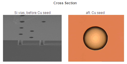
FSM offers Through-Silicon Via (TSV) wafers with a via depth of 100um and a diameter of 50um.
The Through-Silicon Via (TSV) is etched with excellent sidewall surface roughness from the center of the wafer to the edge of the wafer aligned to the notch.
All Through Silicon Vias are etched on a 10 to 100um Via Etch Pattern Layout for a 200mm wafer.
The electroplated copper layer is 10,000 angstroms followed by 2um Cu seed layer and 1000 angstroms Titanium Liner on TEOS.
TSV 1060 SiVia
FSM offers Through-Silicon Via (TSV) wafers with the ability to electrical test vias with diameters of 10um, 20um, 30um, 40um, 45um, 50um, 55um, and 60um.
The Through-Silicon Via (TSV) is etched with excellent sidewall surface roughness from the center of the wafer to the edge of the wafer aligned to the notch.
All Through-Silicon Vias are etched on a 200mm wafer.
The electroplated copper layer is 10,000 angstroms followed by 2um Cu seed layer and 1000 angstroms Titanium Liner on TEOS.
需要请联系FSM
Pattern Wafers
TSV 100 SiVia
TSV 1060 SiVia
TSV 530 SiVia
Packaging Bumped Patterns
Daisy Chain Patterns
Process Capabilities
Etching
Thinning
Bonding
Deposition
TSV 100 SiVia
FSM offers Through-Silicon Via (TSV) wafers with a via depth of 100um and a diameter of 50um.
The Through-Silicon Via (TSV) is etched with excellent sidewall surface roughness from the center of the wafer to the edge of the wafer aligned to the notch.
All Through Silicon Vias are etched on a 10 to 100um Via Etch Pattern Layout for a 200mm wafer.
The electroplated copper layer is 10,000 angstroms followed by 2um Cu seed layer and 1000 angstroms Titanium Liner on TEOS.
TSV 1060 SiVia
FSM offers Through-Silicon Via (TSV) wafers with the ability to electrical test vias with diameters of 10um, 20um, 30um, 40um, 45um, 50um, 55um, and 60um.
The Through-Silicon Via (TSV) is etched with excellent sidewall surface roughness from the center of the wafer to the edge of the wafer aligned to the notch.
All Through-Silicon Vias are etched on a 200mm wafer.
The electroplated copper layer is 10,000 angstroms followed by 2um Cu seed layer and 1000 angstroms Titanium Liner on TEOS.
需要请联系FSM

 简体中文
简体中文 Japanese(日语)
 Korean(韩文)
 English(英文)