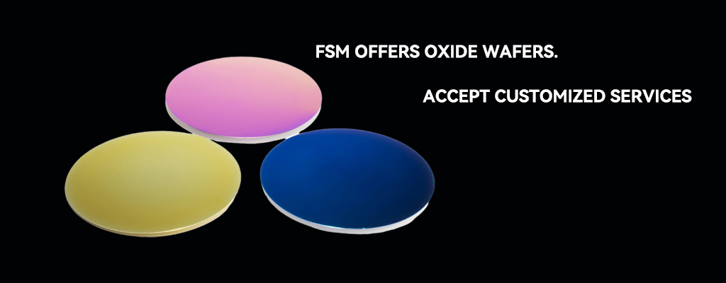
Product Introduction

These are the silicon wafers which have been through either a Wet Thermal Oxide, or a Dry Thermal Oxide process, to “grow” a Thermal Oxide, or Silicon Dioxide (Sio2), layer on the surface of the wafer. This is done by exposing the wafer to a combination of oxidizing agents and heat. The oxide is most commonly used as a dielectric layer and in MEMs devices. Thermal Oxide is grown on both sides of the wafer, but can then be removed from one side if a single side oxide layer is needed.

Parameter Specification

100MM/150MM/200MM/300MM Oxide wafers


200MM 300MM
Thickness 50-50000nm 50-40000nm
Thickness deviation(1 piece) < 3% < 3%
Thickness deviation(More than 2 pieces) < 3% < 3%
Grow Method CZ CZ
Diameter(mm) 200±0.2mm 300±0.2mm
Type P P
Orientation <100> <100>
Resistivity(Ω・cm) 1-100 1-100
Thickness(μm) 725±25 775±25
TTV(μm) ≦25 ≦25
BOW(μm) ≦40 ≦40
WARP(μm) ≦40 ≦40
Surface Metals ≦5.0E 10 atom/cm2 <1 E10 Atoms/cm2


100MM 150MM
Thickness 50-30000nm 50-30000nm
Thickness deviation(1 piece) < 5% < 5%
Thickness deviation(More than 2 pieces) < 5% < 5%
Grow Method CZ CZ
Diameter(mm) 100±0.3mm 150±0.3mm
Type P P
Orientation <100> <100>
Resistivity(Ω・cm) 1-100 1-100
Thickness(μm) 525±25 675±25
TTV(μm) ≦25 ≦25
BOW(μm) ≦40 ≦40
WARP(μm) ≦40 ≦40
Surface Metals ≦5.0E 10 atom/cm2 ≦5.0E 10 atom/cm2

If you have any other needs, please contact us.