Fine Silicon Manufacturing(shanghai) Ltd.(FSM )was established in 2008 and is headquartered in Shanghai's which located in Waigaoqiao Free Trade Zone.FSM is one of the earliest enterprises engaged in silicon wafer processing and sales in China.In 2015, the Japanese branch KOD Corporation was established in Tokyo.At present, FSM Group has two plants in Shanghai and Japan, with a monthly processing capacity of 100,000pcs 12inch silicon wafers.
-
Company Establishment
-
Plant Area
-
Experience
-
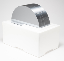
FSM can provide dummy wafers in various sizes from 2 inches to 12 inches, with our own factory to ensure the stable quality and controllable delivery time. We also have various testing equipment to provide parameter testing services as needed.
-
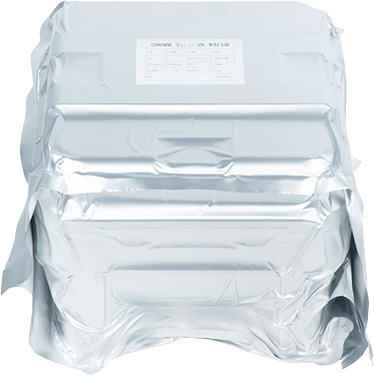
Test grade wafers come right below the prime grade wafers on the quality basis.
-
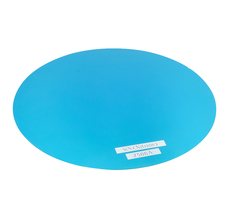
FSM offers silicon thermal oxide wafers.
These are the silicon wafers which have been through either a Wet Thermal Oxide, or a Dry Thermal Oxide process, to “grow” a Thermal Oxide, or Silicon Dioxide (Sio2), layer on the surface of the wafer.
-
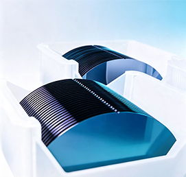
Our SOI (Silicon-On-Insulator) wafers combine a top device silicon layer,buried oxide (BOX) layer, and handle silicon layer, available in diameters from 2" to 8". With tightly controlled thickness tolerances(±5%), low TTV (<5μm) and bow (<20μm), plus flexible doping options(P-type, N-type, intrinsic) and resistivity from 0.001 to over 20,000 Ω·cm, our SOI wafers deliver reliable performance for CMOS,RF, MEMS, and power semiconductor applications.
-
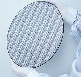
Our GaN (Gallium Nitride) wafers are grown using the Hydride Vapor Phase Epitaxy (HVPE) method, available in semi-insulating (Fe-doped) and N-type (Ge-doped or undoped) variants with C-plane <0001> orientation. These freestanding GaN wafers feature low dislocation density (EPD as low as 1~9E5/cm²), sub-nanometer front surface roughness (Ra ≤0.2nm), and tightly controlled TTV (≤15μm), bow, and warp (≤20μm), making them a high-quality, epi-ready substrate for demanding power and RF device applications.
-
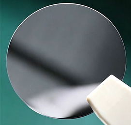
Our InAs (Indium Arsenide) wafers are grown using the Vertical Gradient Freeze (VGF) method, available in 2", 3", and 4" diameters with <100> and <111> orientations. Offered in undoped and doped variants (N-type:S, Sn; P-type: Zn), these epi-ready wafers feature low TTV (≤15μm),bow (≤10μm), and warp (≤15μm) for consistent downstream processing.With polished or etched surface finishes, our InAs wafers are well suited for infrared and high-speed electronic device applications.
-
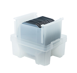
Our InSb (Indium Antimonide) wafers are grown using the Vertical Gradient Freeze (VGF) method, available in 2" and 3" diameters with <100> orientation. Offered in undoped and doped variants (N-type: S,Sn; P-type: Zn), these epi-ready wafers feature tightly controlled TTV (≤15μm), bow (≤15μm), and warp (≤15μm) for consistent downstream processing. With polished or etched surface finishes, our InSb wafers are well suited for infrared detection and sensing applications.
-
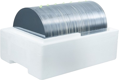
FSM does offer wafer polishing solutions.
2 production bases in the world (Shanghai, Tokyo)

Fine Silicon Manufacturing(shanghai) Ltd.(FSM )was established in 2008 and is headquartered in Shanghai's which located in Waigaoqiao Free Trade Zone.
FSM is one of the earliest enterprises engaged in silicon wafer processing and sales in China.
In 2015, the Japanese branch KOD Corporation was established in Tokyo.
At present, FSM Group has two plants in Shanghai and Japan, with a monthly processing capacity of 100,000pcs 12inch silicon wafers.
At the sales end, FSM, KOD and upstream domestic and oversea wafer makers, wafer reclaim house and downstream semiconductor foundary have stable and good cooperation, customers all over the domestic and foreign countries and regions.
The main business also expanded from single Dummy wafer to the agent of reclaim wafer house, providing wafer reclaim business from 6 -12 inch;
At the same time, we also provide Test and Dummy wafers of various sizes from the wafer maker.
FSM also provides customized coatings wafer in various sizes and film thickness, eg: Thermal oxide, PETEOS, LP-Nitride, PE SiN etc.
In the field of third-generation semiconductors, we are also active and currently offer various sizes of SiC, lithium tantalate/lithium niobate (LiTaO3 (LT) and LiNbO3 (LN)), glass wafers, etc.