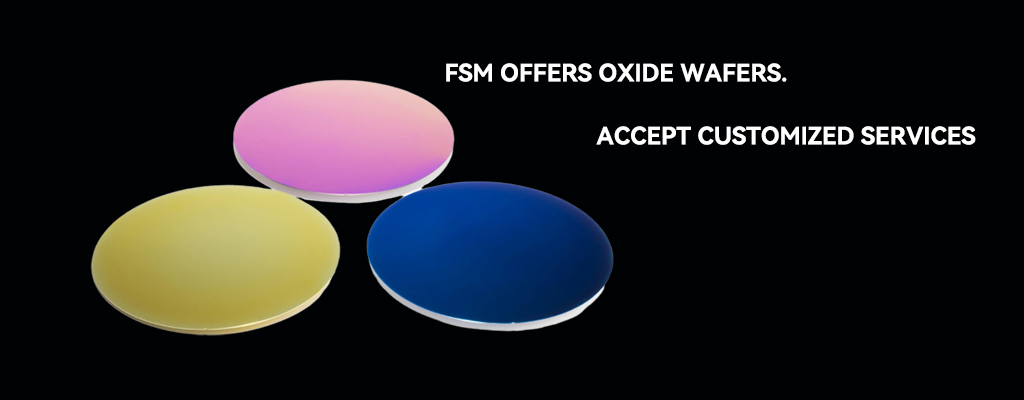
Our InAs (Indium Arsenide) wafers are grown using the Vertical Gradient Freeze (VGF) method, available in 2", 3", and 4" diameters with <100> and <111> orientations. Offered in undoped and doped variants (N-type:S, Sn; P-type: Zn), these epi-ready wafers feature low TTV (≤15μm),bow (≤10μm), and warp (≤15μm) for consistent downstream processing.With polished or etched surface finishes, our InAs wafers are well suited for infrared and high-speed electronic device applications.
Applications
- Infrared photodetectors and lasers
- High-speed, low-power transistors (due to high electron mobility)
- Thermophotovoltaic (TPV) cells
- Quantum well and quantum dot device structures
Why Choose Us?
Grown by the VGF process with comprehensive size coverage (2‑4 inches).
Bow can be controlled within 10 μm, representing a high‑level industry standard.
Multiple types including undoped, N‑type and P‑type are available.
Optional surface polishing or etching treatments, compatible with a wide range of downstream processes.