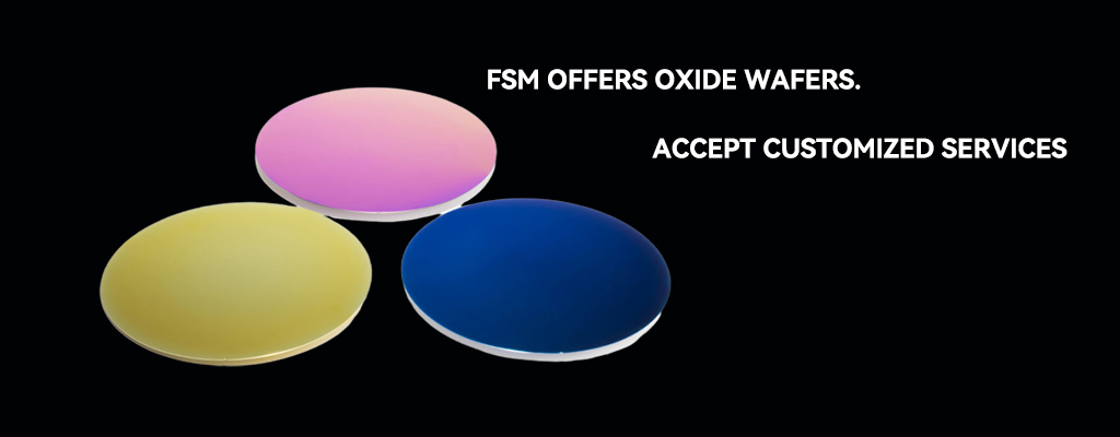
Our Ge (Germanium) wafers are available in diameters from 2" to 6",with thickness options ranging from 175μm to 625μm to suit various process requirements. Offered in undoped, N-type (Sb), and P-type (Gavariants with resistivity from 0.005 to over 30 Ω·cm, these wafers feature <100> and <111> orientations, low TTV/bow/warp (≤25μm), and epi-ready surface finishes. With low etch pit density (<3000/cm²),our Ge wafers provide a reliable substrate for high-efficiency optoelectronic and photovoltaic applications.
Applications
- Substrates for III-V multi-junction solar cells
- Infrared optics and lenses
- Photodetectors and infrared sensors
- Epitaxial growth platform for GaAs and other III-V compound semiconductor devices
Why Choose Us?
Low dislocation density (EPD < 3000/cm²) for stable crystal quality.
Comprehensive thickness specifications (175 μm‑625 μm) to match various product requirements.
TTV, bow and warpage are all controlled within 25 μm.
Suitable for III‑V group epitaxial growth, making it an ideal substrate for high‑efficiency solar cells.