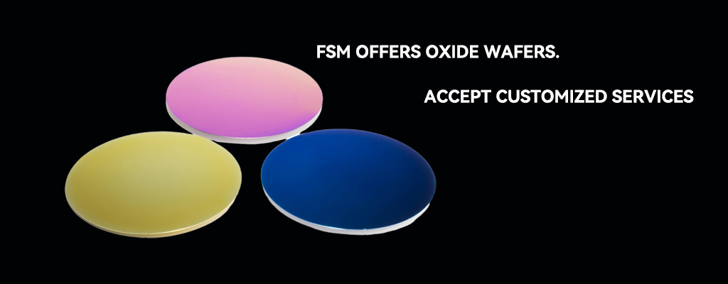
Our InSb (Indium Antimonide) wafers are grown using the Vertical Gradient Freeze (VGF) method, available in 2" and 3" diameters with <100> orientation. Offered in undoped and doped variants (N-type: S,Sn; P-type: Zn), these epi-ready wafers feature tightly controlled TTV (≤15μm), bow (≤15μm), and warp (≤15μm) for consistent downstream processing. With polished or etched surface finishes, our InSb wafers are well suited for infrared detection and sensing applications.
Applications
- Infrared detectors and focal plane arrays
- Hall effect sensors and magnetoresistive devices
- Thermal imaging systems
- High-speed, low-power electronic devices
Why Choose Us?
Grown by the VGF process for excellent material consistency.
TTV, bow and warpage are all controlled within 15 μm.
Optional surface polishing or etching treatments to satisfy diverse process requirements.
Specialized in narrow‑bandgap material production, ideal for high‑precision infrared device applications.