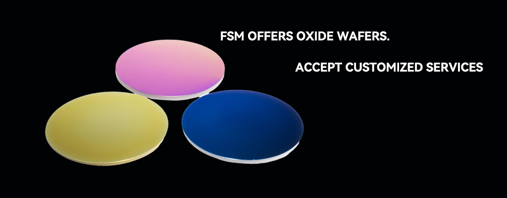
Our InP (Indium Phosphide) wafers are grown using the Vertical Gradient Freeze (VGF) method, available in 2", 3", and 4" sizes with <100> orientation. Offered in undoped and doped variants (N-type: S, Sn;P-type: Zn), these epi-ready wafers feature low TTV (≤15μm), bow (≤15μm), and warp (≤15μm) for consistent downstream epitaxial growth.With polished or etched surface options, our InP wafers are well suited for photonic and optoelectronic device fabrication.
Applications
- Laser diodes and photodetectors for optical communication
- High-frequency and high-electron-mobility transistors (HEMT/HBT)
- Photonic integrated circuits
- Solar cell substrates for multi-junction cells
Why Choose Us?
Grown by the VGF process with stable crystal quality.
Undoped, N‑type and P‑type doping options are available to meet diverse device‑design requirements.
TTV, bow and warpage are all controlled within 15 μm to guarantee consistent epitaxial growth.
Surfaces meet epitaxial‑grade standards and can be directly applied in downstream processes.